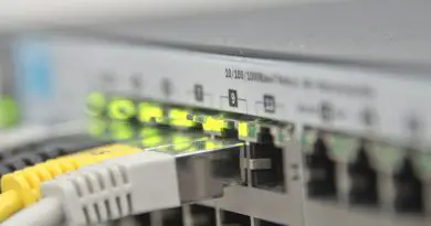
Signal Integrity in High-Speed PCB Design
An advanced electronics project may not always perform as expected, especially when it comes to high-speed PCB.
Issues that usually arise include distorted signals or heaps of data errors, and it is difficult to make sense of why they are happening. This scenario highlights the importance of signal integrity, particularly in projects like high-speed PCB design creation.
What is Signal Integrity?
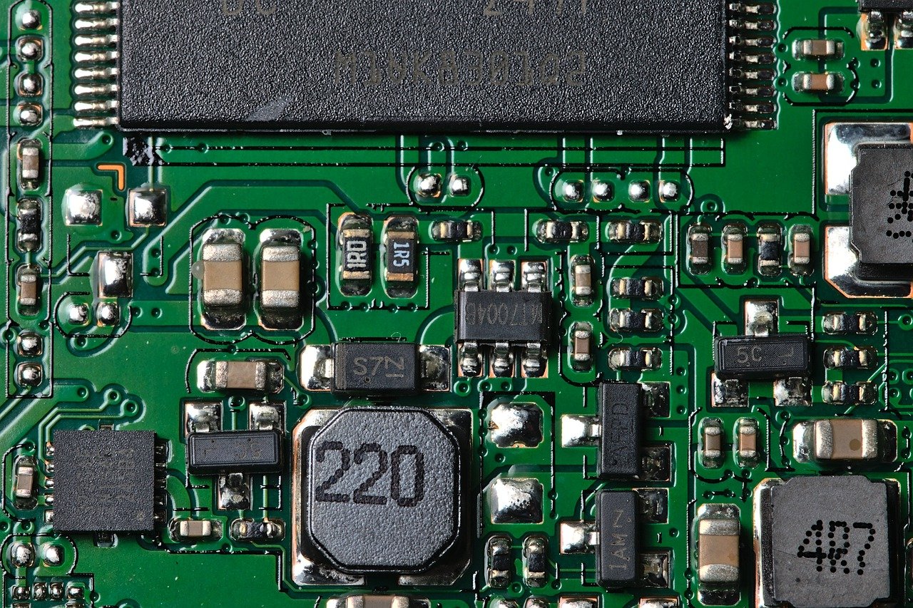
Signal integrity ensures electrical signals maintain their quality as they travel through a printed circuit board. In high-speed PCB designs, signals degrade due to reflection, crosstalk, and electromagnetic interference (EMI). Consider maintaining signal integrity for these projects.
Factors That Affect Signal Integrity
Impedance Matching
If you run water through a series of pipes, but the pipes are of different sizes, the water flow would be inconsistent. The same concept applies to electrical signals. Mismatched impedance can cause reflections, distorting the signals. Keeping impedance consistent throughout the PCB
helps minimize these reflections.
Trace Length and Layout
Think of trace length as the distance a runner has to cover. Longer traces can delay signals, just like longer distances slow down runners. Proper routing and keeping trace lengths short help maintain signal integrity.
Crosstalk
Overheard another nearby conversation that interfered with your phone call? That’s similar to crosstalk in PCBs, where a signal in one trace interferes with a signal in another. Keeping traces adequately spaced apart helps reduce this interference.
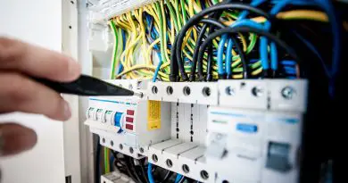
Ground Planes and Power Delivery
A solid ground plane is like a reliable foundation for a building, providing a return path for signals and reducing noise and EMI. Proper power delivery ensures that components receive clean, stable power, which is essential for maintaining signal integrity.
Via Usage:
Vias are like the bridges between different layers of a PCB. However, too many vias can introduce unwanted electrical characteristics, degrading signal quality. Minimizing vias and placing them strategically helps maintain signal integrity.
Practical Tips for Maintaining Signal Integrity
Consistent Impedance Control
Use tools and calculators to ensure trace impedance is consistent. This practice is similar to making sure all the pipes in our water flow analogy are of the same diameter.
Optimal Trace Routing
Route high-speed signals using the shortest and most direct paths. Avoid sharp bends and keep trace lengths equal for differential pairs to minimize signal skew. Think of it as plotting the most efficient route for a racecourse.
Effective Crosstalk Mitigation
Increase the spacing between traces and use guard traces where necessary. For differential pairs,
maintain consistent spacing and route them closely together. It’s like ensuring that two runners
stay in their lanes to avoid bumping into each other.
Robust Ground Plane Design
Ensure a continuous ground plane for a low-impedance return path. Avoid splitting the ground plane to prevent noise issues. It’s like having a solid foundation for a house, ensuring stability and support.
Careful Via Management
Minimize the number of vias in high-speed signal paths. When necessary, place them strategically to reduce their impact. It’s akin to building bridges only where essential to maintain a smooth journey.
Power Integrity Considerations
Design power delivery networks (PDNs) that provide clean and stable power. Use decoupling capacitors near power pins to filter out noise and stabilize the power supply. Think of it as using surge protectors to ensure your electronic devices receive stable power.
Simulation and Testing
Utilize simulation tools to model and analyze signal integrity before manufacturing the PCB. Tools like SPICE, HyperLynx, and ADS can help identify some issues. After the PCB fabrication, signal integrity testing using oscilloscopes and network analyzers can validate the design.
Advanced Techniques for High-Speed PCB Design
Differential Signaling
Differential signaling uses two complementary signals to transmit data. This technique is less susceptible to noise and EMI, making it ideal for high-speed designs. Ensure that differential pairs are routed closely together with equal trace lengths to maintain signal integrity.
Controlled Impedance Traces
For high-speed signals, use controlled impedance traces to ensure consistent impedance throughout the signal path. This involves specifying the trace width, spacing, and the dielectric properties of the PCB material.
Signal Layer Stack-Up
Design the PCB layer stack-up to optimize signal integrity. Place high-speed signal layers adjacent to ground planes to reduce noise and provide a clear return path. Use alternating signal and ground layers to minimize crosstalk.
Advanced Materials
Consider using advanced PCB materials with low dielectric loss and high thermal stability for high-speed designs. These materials can help maintain signal integrity by reducing signal attenuation and distortion.
Termination Techniques
Implement termination techniques, such as series or parallel termination, to match the impedance of the signal source and load. Proper termination reduces reflections and improves signal integrity.

Aric is a tech enthusiast , who love to write about the tech related products and ‘How To’ blogs . IT Engineer by profession , right now working in the Automation field in a Software product company . The other hobbies includes singing , trekking and writing blogs .